Development boards
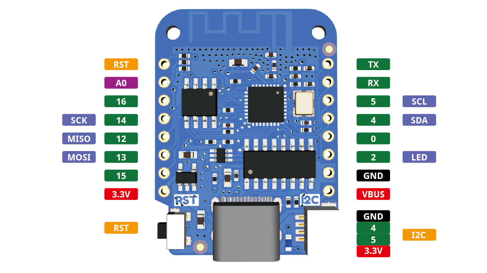
LOLIN D1 mini v4.0.0 pinout
ESP8266EX · USB-C · I²C connector
Open in the interactive atlas →See the pin map, choose functions and save a wiring plan.Türkçe
At a glance
- Platform / manufacturer
- Espressif
- Type
- Development boards
- MCU
- ESP8266EX
- Physical contacts
- 20
- GPIO
- 11
- I/O voltage
- 3.3 V I/O
- Interfaces (pin count)
- I²C (4) · SPI (4) · UART (5) · ADC (1) · PWM (12) · IRQ (13) · SYSTEM (2)
- MCU / processor core
- 1 × Tensilica L106 32-bit [a]
- Clock speed / maximum
- 80 MHz (160 MHz max) [a]
- Internal RAM / system RAM
- 80 KB user data SRAM + 32 KB instruction RAM + 32 KB instruction cache [a]
- Pin sources checked
- 2026-11-19
- Technical details reviewed
- 2026-11-19
All pins (20)
| Physical | Pin name | Type | Functions | Notes and warnings | Source |
|---|---|---|---|---|---|
| J2.1 | RST | System | — | — | [1] [2] |
| J2.2 | A0 | Analog | ADC0 | A0 connects to ESP8266 TOUT through the 220 kΩ and 100 kΩ divider in the schematic. Source: [1] | [1] [2] |
| J2.3 | D0 | General-purpose I/O | WAKEGPIO interrupt | — | [1] [2] |
| J2.4 | D5 | General-purpose I/O | HSPI SCKPWMGPIO interrupt | — | [1] [2] |
| J2.5 | D6 | General-purpose I/O | HSPI MISOPWMGPIO interrupt | — | [1] [2] |
| J2.6 | D7 | General-purpose I/O | HSPI MOSIUART0 CTSPWMGPIO interrupt | — | [1] [2] |
| J2.7 | D8 | General-purpose I/O | HSPI CSUART0 RTSPWMGPIO interrupt | Strapping pin: its reset-time level affects boot or hardware configuration. Check that external circuitry preserves the required reset levels. This GPIO is one of the ESP8266 pins sampled for boot mode at reset. Source: [1] | [1] [2] |
| J2.8 | 3V3 | Power | — | — | [1] [2] |
| J3.1 | TX | General-purpose I/O | UART0 TXPWMGPIO interrupt | — | [1] [2] |
| J3.2 | RX | General-purpose I/O | UART0 RXPWMGPIO interrupt | — | [1] [2] |
| J3.3 | D1 | General-purpose I/O | I2C SCLPWMGPIO interrupt | Same electrical signal as P1.3 | [1] [2] |
| J3.4 | D2 | General-purpose I/O | I2C SDAPWMGPIO interrupt | Same electrical signal as P1.2 | [1] [2] |
| J3.5 | D3 | General-purpose I/O | FLASH buttonPWMGPIO interrupt | Strapping pin: its reset-time level affects boot or hardware configuration. Check that external circuitry preserves the required reset levels. This GPIO is one of the ESP8266 pins sampled for boot mode at reset. Source: [1] | [1] [2] |
| J3.6 | D4 | General-purpose I/O | UART1 TXPWMGPIO interrupt | Strapping pin: its reset-time level affects boot or hardware configuration. Check that external circuitry preserves the required reset levels. GPIO2 (D4) shares the on-board LED and sets a boot level at reset. Source: [1] | [1] [2] |
| J3.7 | GND | Ground | — | — | [1] [2] |
| J3.8 | 5V | Power | — | — | [1] [2] |
| P1.1 | GND | Ground | — | — | [1] [2] |
| P1.2 | SDA | General-purpose I/O | I2C SDAPWMGPIO interrupt | Same electrical signal as J3.4 | [1] [2] |
| P1.3 | SCL | General-purpose I/O | I2C SCLPWMGPIO interrupt | Same electrical signal as J3.3 | [1] [2] |
| P1.4 | 3V3 | Power | — | — | [1] [2] |
Sources
Pin and warning references
- LOLIN D1 mini v4.0.0 schematic · PDF p. 1LOLIN D1 mini v4.0.0 · J2/J3/P1, A0 divider, LED and boot resistors
- LOLIN D1 mini v4.0.0 top-view pinoutWEMOS v4.0.0 top view · USB at the bottom and P1 at right
Technical sources (3)
- ESP8266EX DatasheetEspressif Systems · Locked pin-source document; see sources/manifest.json for revision and SHA-256
- LOLIN D1 mini v4.0.0WEMOS · Technical specifications, schematic and revision
- LOLIN D1 mini v4.0.0 schematicWEMOS · Locked schematic or pin-source document
Locked source documents
- ESP8266EX DatasheetEspressif Systems · v7.1 · 2025-11
- LOLIN D1 mini v4.0.0 schematicWEMOS · 4.0.0
- LOLIN D1 mini v4.0.0 top-view pinoutWEMOS · 4.0.0