Development boards
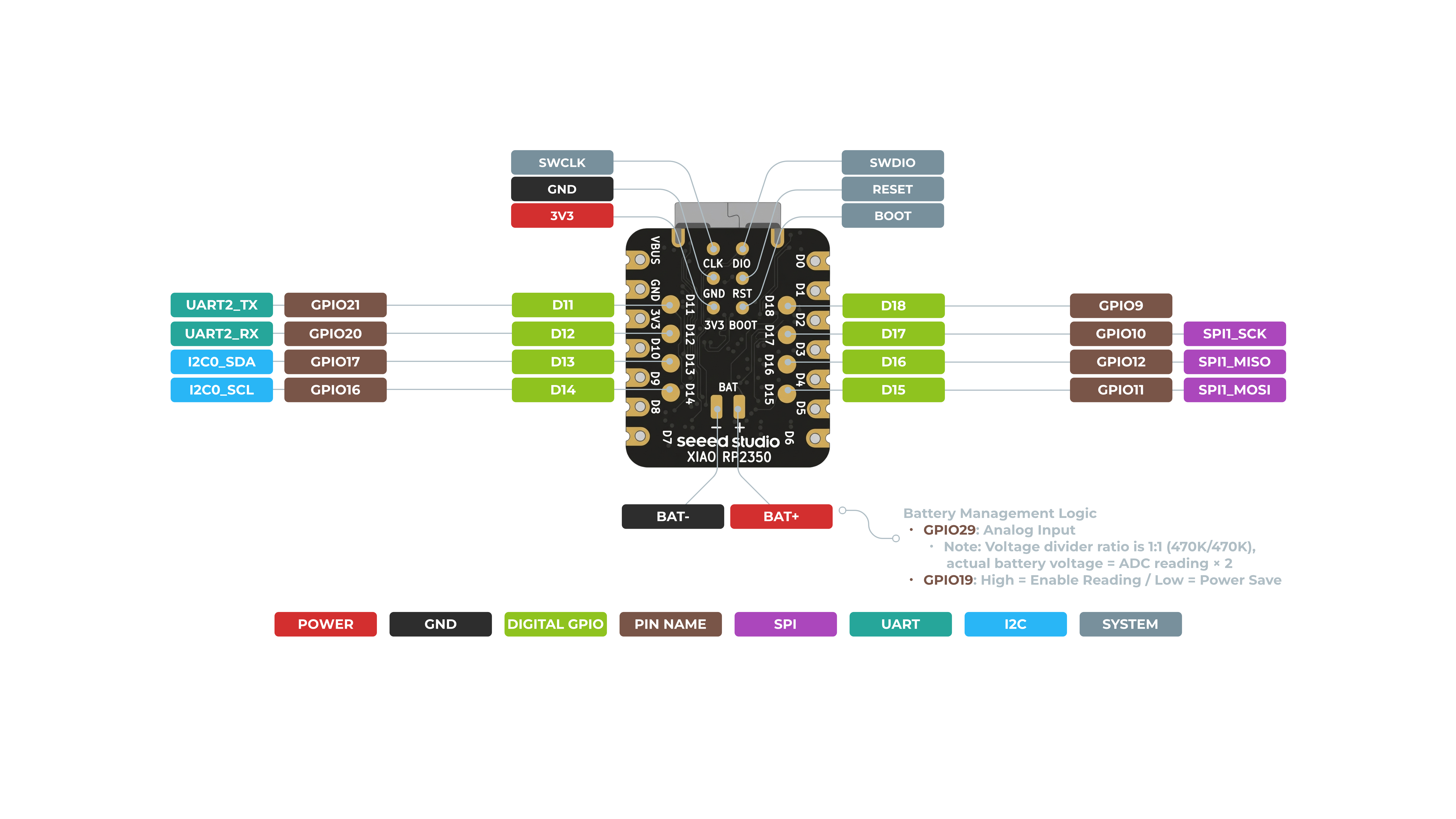
Seeed Studio XIAO RP2350 pinout
RP2350A · side headers and back pads
Open in the interactive atlas →See the pin map, choose functions and save a wiring plan.Türkçe
At a glance
- Platform / manufacturer
- Seeed Studio
- Type
- Development boards
- MCU
- RP2350A
- Physical contacts
- 22
- GPIO
- 19
- I/O voltage
- 3.3 V I/O
- Interfaces (pin count)
- I²C (19) · SPI (19) · UART (19) · USB (19) · ADC (3) · PWM (19) · CLOCK (8) · HSTX (3) · PIO (19) · QMI (1) · SIO (19)
- MCU / processor core
- 2 × Arm Cortex-M33 / 2 × Hazard3 RISC-V [a]
- Clock speed / maximum
- 150 MHz [a]
- Internal RAM / system RAM
- 520 KB SRAM [a]
- Fixed ROM / boot ROM
- 32 KB boot ROM [a]
- Pin sources checked
- 2026-11-19
- Technical details reviewed
- 2026-11-19
Cautions for this board
- D11–D18 are solder pads on the back of the board. The map shows them as a separate connection group. Source: [1]
- RP2350-E9 (A2 stepping): a Bank 0 GPIO configured as an input can be held at about 2.2 V by pad leakage while its voltage is in the undefined logic region; the internal pull-down is too weak to overcome it. Pull or drive the line low with 8.2 kΩ or less; the pull-up still works. Source: [2]
All pins (22)
| Physical | Pin name | Type | Functions | Notes and warnings | Source |
|---|---|---|---|---|---|
| L.1 | D0MCU pin 40 | General-purpose I/O | SPI1 SCK F1UART1 CTS F2I2C1 SDA F3PWM5 A F4SIO F5PIO0 F6PIO1 F7PIO2 F8USB VBUS EN F10UART1 TX F11ADC0 | Non-FT ADC/GPIO RP2350-E9 (A2 stepping): a Bank 0 GPIO configured as an input can be held at about 2.2 V by pad leakage while its voltage is in the undefined logic region; the internal pull-down is too weak to overcome it. Pull or drive the line low with 8.2 kΩ or less; the pull-up still works. Source: [2] | [1] [3] [4] [2] |
| L.2 | D1MCU pin 41 | General-purpose I/O | SPI1 TX F1UART1 RTS F2I2C1 SCL F3PWM5 B F4SIO F5PIO0 F6PIO1 F7PIO2 F8USB OVCUR DET F10UART1 RX F11ADC1 | Non-FT ADC/GPIO RP2350-E9 (A2 stepping): a Bank 0 GPIO configured as an input can be held at about 2.2 V by pad leakage while its voltage is in the undefined logic region; the internal pull-down is too weak to overcome it. Pull or drive the line low with 8.2 kΩ or less; the pull-up still works. Source: [2] | [1] [3] [4] [2] |
| L.3 | D2MCU pin 42 | General-purpose I/O | SPI1 RX F1UART0 TX F2I2C0 SDA F3PWM6 A F4SIO F5PIO0 F6PIO1 F7PIO2 F8USB VBUS DET F10ADC2 | Non-FT ADC/GPIO RP2350-E9 (A2 stepping): a Bank 0 GPIO configured as an input can be held at about 2.2 V by pad leakage while its voltage is in the undefined logic region; the internal pull-down is too weak to overcome it. Pull or drive the line low with 8.2 kΩ or less; the pull-up still works. Source: [2] | [1] [3] [4] [2] |
| L.4 | D3MCU pin 8 | General-purpose I/O | SPI0 CSn F1UART1 RX F2I2C0 SCL F3PWM2 B F4SIO F5PIO0 F6PIO1 F7PIO2 F8TRACEDATA3 F9USB VBUS EN F10 | Conditional 5.5V input RP2350-E9 (A2 stepping): a Bank 0 GPIO configured as an input can be held at about 2.2 V by pad leakage while its voltage is in the undefined logic region; the internal pull-down is too weak to overcome it. Pull or drive the line low with 8.2 kΩ or less; the pull-up still works. Source: [2] | [1] [3] [4] [2] |
| L.5 | D4MCU pin 9 | General-purpose I/O | SPI0 SCK F1UART1 CTS F2I2C1 SDA F3PWM3 A F4SIO F5PIO0 F6PIO1 F7PIO2 F8USB OVCUR DET F10UART1 TX F11 | Conditional 5.5V input RP2350-E9 (A2 stepping): a Bank 0 GPIO configured as an input can be held at about 2.2 V by pad leakage while its voltage is in the undefined logic region; the internal pull-down is too weak to overcome it. Pull or drive the line low with 8.2 kΩ or less; the pull-up still works. Source: [2] | [1] [3] [4] [2] |
| L.6 | D5MCU pin 10 | General-purpose I/O | SPI0 TX F1UART1 RTS F2I2C1 SCL F3PWM3 B F4SIO F5PIO0 F6PIO1 F7PIO2 F8USB VBUS DET F10UART1 RX F11 | Conditional 5.5V input RP2350-E9 (A2 stepping): a Bank 0 GPIO configured as an input can be held at about 2.2 V by pad leakage while its voltage is in the undefined logic region; the internal pull-down is too weak to overcome it. Pull or drive the line low with 8.2 kΩ or less; the pull-up still works. Source: [2] | [1] [3] [4] [2] |
| L.7 | D6MCU pin 2 | General-purpose I/O | SPI0 RX F1UART0 TX F2I2C0 SDA F3PWM0 A F4SIO F5PIO0 F6PIO1 F7PIO2 F8QMI CS1n F9USB OVCUR DET F10 | Conditional 5.5V input RP2350-E9 (A2 stepping): a Bank 0 GPIO configured as an input can be held at about 2.2 V by pad leakage while its voltage is in the undefined logic region; the internal pull-down is too weak to overcome it. Pull or drive the line low with 8.2 kΩ or less; the pull-up still works. Source: [2] | [1] [3] [4] [2] |
| R.1 | 5V | Power | — | — | [1] |
| R.2 | GND | Ground | — | — | [1] |
| R.3 | 3V3 | Power | — | — | [1] |
| R.4 | D10MCU pin 5 | General-purpose I/O | SPI0 TX F1UART0 RTS F2I2C1 SCL F3PWM1 B F4SIO F5PIO0 F6PIO1 F7PIO2 F8TRACEDATA1 F9USB OVCUR DET F10UART0 RX F11 | Conditional 5.5V input RP2350-E9 (A2 stepping): a Bank 0 GPIO configured as an input can be held at about 2.2 V by pad leakage while its voltage is in the undefined logic region; the internal pull-down is too weak to overcome it. Pull or drive the line low with 8.2 kΩ or less; the pull-up still works. Source: [2] | [1] [3] [4] [2] |
| R.5 | D9MCU pin 7 | General-purpose I/O | SPI0 RX F1UART1 TX F2I2C0 SDA F3PWM2 A F4SIO F5PIO0 F6PIO1 F7PIO2 F8TRACEDATA2 F9USB VBUS DET F10 | Conditional 5.5V input RP2350-E9 (A2 stepping): a Bank 0 GPIO configured as an input can be held at about 2.2 V by pad leakage while its voltage is in the undefined logic region; the internal pull-down is too weak to overcome it. Pull or drive the line low with 8.2 kΩ or less; the pull-up still works. Source: [2] | [1] [3] [4] [2] |
| R.6 | D8MCU pin 4 | General-purpose I/O | SPI0 SCK F1UART0 CTS F2I2C1 SDA F3PWM1 A F4SIO F5PIO0 F6PIO1 F7PIO2 F8TRACEDATA0 F9USB VBUS EN F10UART0 TX F11 | Conditional 5.5V input RP2350-E9 (A2 stepping): a Bank 0 GPIO configured as an input can be held at about 2.2 V by pad leakage while its voltage is in the undefined logic region; the internal pull-down is too weak to overcome it. Pull or drive the line low with 8.2 kΩ or less; the pull-up still works. Source: [2] | [1] [3] [4] [2] |
| R.7 | D7MCU pin 3 | General-purpose I/O | SPI0 CSn F1UART0 RX F2I2C0 SCL F3PWM0 B F4SIO F5PIO0 F6PIO1 F7PIO2 F8TRACECLK F9USB VBUS DET F10 | Conditional 5.5V input RP2350-E9 (A2 stepping): a Bank 0 GPIO configured as an input can be held at about 2.2 V by pad leakage while its voltage is in the undefined logic region; the internal pull-down is too weak to overcome it. Pull or drive the line low with 8.2 kΩ or less; the pull-up still works. Source: [2] | [1] [3] [4] [2] |
| TP.16 | D11MCU pin 33 | General-purpose I/O | SPI0 CSn F1UART1 RX F2I2C0 SCL F3PWM2 B F4SIO F5PIO0 F6PIO1 F7PIO2 F8CLOCK GPOUT0 F9USB OVCUR DET F10 | Conditional 5.5V input RP2350-E9 (A2 stepping): a Bank 0 GPIO configured as an input can be held at about 2.2 V by pad leakage while its voltage is in the undefined logic region; the internal pull-down is too weak to overcome it. Pull or drive the line low with 8.2 kΩ or less; the pull-up still works. Source: [2] | [5] [1] [3] [4] [2] |
| TP.15 | D12MCU pin 32 | General-purpose I/O | SPI0 RX F1UART1 TX F2I2C0 SDA F3PWM2 A F4SIO F5PIO0 F6PIO1 F7PIO2 F8CLOCK GPIN0 F9USB VBUS EN F10 | Conditional 5.5V input RP2350-E9 (A2 stepping): a Bank 0 GPIO configured as an input can be held at about 2.2 V by pad leakage while its voltage is in the undefined logic region; the internal pull-down is too weak to overcome it. Pull or drive the line low with 8.2 kΩ or less; the pull-up still works. Source: [2] | [5] [1] [3] [4] [2] |
| TP.14 | D13MCU pin 28 | General-purpose I/O | HSTX F0SPI0 CSn F1UART0 RX F2I2C0 SCL F3PWM0 B F4SIO F5PIO0 F6PIO1 F7PIO2 F8USB VBUS EN F10 | Conditional 5.5V input RP2350-E9 (A2 stepping): a Bank 0 GPIO configured as an input can be held at about 2.2 V by pad leakage while its voltage is in the undefined logic region; the internal pull-down is too weak to overcome it. Pull or drive the line low with 8.2 kΩ or less; the pull-up still works. Source: [2] | [5] [1] [3] [4] [2] |
| TP.13 | D14MCU pin 27 | General-purpose I/O | HSTX F0SPI0 RX F1UART0 TX F2I2C0 SDA F3PWM0 A F4SIO F5PIO0 F6PIO1 F7PIO2 F8USB VBUS DET F10 | Conditional 5.5V input RP2350-E9 (A2 stepping): a Bank 0 GPIO configured as an input can be held at about 2.2 V by pad leakage while its voltage is in the undefined logic region; the internal pull-down is too weak to overcome it. Pull or drive the line low with 8.2 kΩ or less; the pull-up still works. Source: [2] | [5] [1] [3] [4] [2] |
| TP.12 | D18MCU pin 13 | General-purpose I/O | SPI1 CSn F1UART1 RX F2I2C0 SCL F3PWM4 B F4SIO F5PIO0 F6PIO1 F7PIO2 F8USB OVCUR DET F10 | Conditional 5.5V input RP2350-E9 (A2 stepping): a Bank 0 GPIO configured as an input can be held at about 2.2 V by pad leakage while its voltage is in the undefined logic region; the internal pull-down is too weak to overcome it. Pull or drive the line low with 8.2 kΩ or less; the pull-up still works. Source: [2] | [5] [1] [3] [4] [2] |
| TP.11 | D17MCU pin 14 | General-purpose I/O | SPI1 SCK F1UART1 CTS F2I2C1 SDA F3PWM5 A F4SIO F5PIO0 F6PIO1 F7PIO2 F8USB VBUS DET F10UART1 TX F11 | Conditional 5.5V input RP2350-E9 (A2 stepping): a Bank 0 GPIO configured as an input can be held at about 2.2 V by pad leakage while its voltage is in the undefined logic region; the internal pull-down is too weak to overcome it. Pull or drive the line low with 8.2 kΩ or less; the pull-up still works. Source: [2] | [5] [1] [3] [4] [2] |
| TP.8 | D16MCU pin 16 | General-purpose I/O | HSTX F0SPI1 RX F1UART0 TX F2I2C0 SDA F3PWM6 A F4SIO F5PIO0 F6PIO1 F7PIO2 F8CLOCK GPIN0 F9USB OVCUR DET F10 | Conditional 5.5V input RP2350-E9 (A2 stepping): a Bank 0 GPIO configured as an input can be held at about 2.2 V by pad leakage while its voltage is in the undefined logic region; the internal pull-down is too weak to overcome it. Pull or drive the line low with 8.2 kΩ or less; the pull-up still works. Source: [2] | [5] [1] [3] [4] [2] |
| TP.7 | D15MCU pin 15 | General-purpose I/O | SPI1 TX F1UART1 RTS F2I2C1 SCL F3PWM5 B F4SIO F5PIO0 F6PIO1 F7PIO2 F8USB VBUS EN F10UART1 RX F11 | Conditional 5.5V input RP2350-E9 (A2 stepping): a Bank 0 GPIO configured as an input can be held at about 2.2 V by pad leakage while its voltage is in the undefined logic region; the internal pull-down is too weak to overcome it. Pull or drive the line low with 8.2 kΩ or less; the pull-up still works. Source: [2] | [5] [1] [3] [4] [2] |
Model-specific features and connection notes
- Two cores run concurrently; all four cores cannot run together. 12 PIO state machines. [a]
Sources
Pin and warning references
- Seeed Studio XIAO RP2350 schematic · PDF p. 5XIAO side headers · D0–D10 and power · RP2350 expansion pads when fitted to this design
- RP2350 Datasheet · PDF p. 1359Appendix D.5.1 · RP2350-E9 · increased leakage on Bank 0 GPIO inputs (A2 stepping; pp. 1359–1360)
- RP2350 Datasheet · PDF p. 1333§14.8.2.2 · Tables 1674–1679 · package pin list
- RP2350 Datasheet · PDF p. 1332§14.8.2.1 · Table 1673 · FT input conditions; pin types in Tables 1674–1679
- Seeed Studio XIAO RP2350 back viewRear view · D11–D18 pad positions
Technical sources (3)
- RP2350 DatasheetManufacturer · Locked pin-source document; see sources/manifest.json for revision and SHA-256
- XIAO RP2350 hardware guideSeeed Studio · Specifications, pin map and battery connection
- Seeed Studio XIAO RP2350 schematicSeeed Studio · Locked schematic or pin-source document
Locked source documents
- RP2350 DatasheetRelease 8 · 2026-10-01
- Seeed Studio XIAO RP2350 schematicSeeed Studio · v1.0
- Seeed Studio XIAO RP2350 back viewSeeed Studio · v1.0 drawing