Development boards
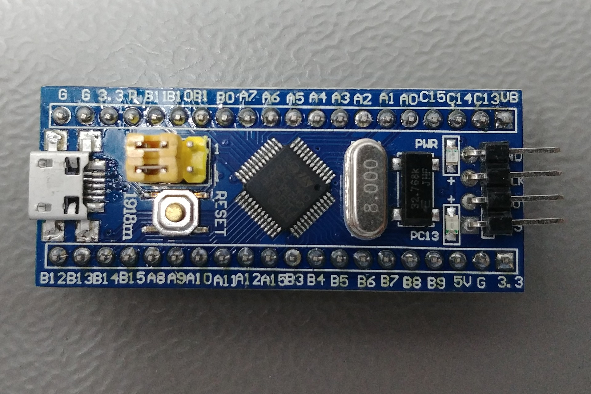
STM32 Blue Pill pinout
STM32F103C8T6 · 2 × 20 header + 4 SWD pins
Open in the interactive atlas →See the pin map, choose functions and save a wiring plan.Türkçe
Board pins follow a community reference; MCU functions follow ST documentation. Check chip markings and wiring on clones. With USB at the top: H2 left, H1 right, SWD below. H1/H2/SWD positions are not chip pin numbers. Oscillators, LED, USB and debug lines share board circuitry. AFIO remap settings apply to whole peripherals; configure selected pins consistently.
At a glance
- Platform / manufacturer
- STM32
- Type
- Development boards
- MCU
- STM32F103C8T6
- Physical contacts
- 44
- GPIO
- 34
- I/O voltage
- 3.3 V I/O
- Interfaces (pin count)
- I²C (8) · SPI (12) · UART (17) · CAN (4) · USB (2) · ADC (10) · PWM (25) · CLOCK (3) · JTAG (5) · SWD (2) · SYSTEM (2) · TIMER (3)
- Power and logic level
- Board GPIO: 3.3 V. Select USB / external power using the jumper and bridge conditions in the board manual. [a] [b] [c]
- MCU datasheet initial publication
- 2007-06-01 [b]
- Pin sources checked
- 2026-11-05
- Technical details reviewed
- 2026-11-14
All pins (44)
| Physical | Pin name | Type | Functions | Notes and warnings | Source |
|---|---|---|---|---|---|
| H1.1 | VBATMCU pin 1 | Power | — | Backup-domain supply. Check the ST datasheet for permitted voltage and power sequencing. | [1] [2] [3] [4] [5] |
| H1.2 | PC13MCU pin 2 | General-purpose I/O | TAMPER-RTC | 3.3V Only PC13 drives the active-low user LED. ST’s PC13–PC15 limits apply: 3 mA, 2 MHz, 30 pF; do not use it as a current source. | [1] [2] [3] [4] [5] [6] |
| H1.3 | PC14MCU pin 3 | General-purpose I/O | OSC32_IN | 3.3V Only Connected to the board’s 32.768 kHz LSE crystal. GPIO use can be affected by the crystal circuit; PC13–PC15 low-drive limits apply. | [1] [2] [3] [4] [5] [6] |
| H1.4 | PC15MCU pin 4 | General-purpose I/O | OSC32_OUT | 3.3V Only Connected to the board’s 32.768 kHz LSE crystal. GPIO use can be affected by the crystal circuit; PC13–PC15 low-drive limits apply. | [1] [2] [3] [4] [5] [6] |
| H1.5 | PA0MCU pin 10 | General-purpose I/O | WKUPUSART2_CTS USART2_REMAP=0 USART2_REMAP: 0ADC12_IN0TIM2_CH1_ETR TIM2_REMAP=00|10 TIM2_REMAP: 00 / 10 | 3.3V Only | [1] [2] [3] [4] [7] [6] |
| H1.6 | PA1MCU pin 11 | General-purpose I/O | USART2_RTS USART2_REMAP=0 USART2_REMAP: 0ADC12_IN1TIM2_CH2 TIM2_REMAP=00|10 TIM2_REMAP: 00 / 10 | 3.3V Only | [1] [2] [3] [4] [7] [6] |
| H1.7 | PA2MCU pin 12 | General-purpose I/O | USART2_TX USART2_REMAP=0 USART2_REMAP: 0ADC12_IN2TIM2_CH3 TIM2_REMAP=00|01 TIM2_REMAP: 00 / 01 | 3.3V Only | [1] [2] [3] [4] [7] [6] |
| H1.8 | PA3MCU pin 13 | General-purpose I/O | USART2_RX USART2_REMAP=0 USART2_REMAP: 0ADC12_IN3TIM2_CH4 TIM2_REMAP=00|01 TIM2_REMAP: 00 / 01 | 3.3V Only | [1] [2] [3] [4] [7] [6] |
| H1.9 | PA4MCU pin 14 | General-purpose I/O | SPI1_NSS SPI1_REMAP=0 SPI1_REMAP: 0USART2_CK USART2_REMAP=0 USART2_REMAP: 0ADC12_IN4 | 3.3V Only | [1] [2] [3] [4] [7] [6] |
| H1.10 | PA5MCU pin 15 | General-purpose I/O | SPI1_SCK SPI1_REMAP=0 SPI1_REMAP: 0ADC12_IN5 | 3.3V Only | [1] [2] [3] [4] [7] [6] |
| H1.11 | PA6MCU pin 16 | General-purpose I/O | SPI1_MISO SPI1_REMAP=0 SPI1_REMAP: 0ADC12_IN6TIM3_CH1 TIM3_REMAP=00 TIM3_REMAP: 00TIM1_BKIN TIM1_REMAP=01 TIM1_REMAP: 01 | 3.3V Only | [1] [2] [3] [4] [7] [6] |
| H1.12 | PA7MCU pin 17 | General-purpose I/O | SPI1_MOSI SPI1_REMAP=0 SPI1_REMAP: 0ADC12_IN7TIM3_CH2 TIM3_REMAP=00 TIM3_REMAP: 00TIM1_CH1N TIM1_REMAP=01 TIM1_REMAP: 01 | 3.3V Only | [1] [2] [3] [4] [7] [6] |
| H1.13 | PB0MCU pin 18 | General-purpose I/O | ADC12_IN8TIM3_CH3 TIM3_REMAP=00|10 TIM3_REMAP: 00 / 10TIM1_CH2N TIM1_REMAP=01 TIM1_REMAP: 01 | 3.3V Only | [1] [2] [3] [4] [7] [6] |
| H1.14 | PB1MCU pin 19 | General-purpose I/O | ADC12_IN9TIM3_CH4 TIM3_REMAP=00|10 TIM3_REMAP: 00 / 10TIM1_CH3N TIM1_REMAP=01 TIM1_REMAP: 01 | 3.3V Only | [1] [2] [3] [4] [7] [6] |
| H1.15 | PB10MCU pin 21 | General-purpose I/O | I2C2_SCLUSART3_TX USART3_REMAP=00 USART3_REMAP: 00TIM2_CH3 TIM2_REMAP=10|11 TIM2_REMAP: 10 / 11 | 5V FT | [1] [2] [3] [4] [8] [6] |
| H1.16 | PB11MCU pin 22 | General-purpose I/O | I2C2_SDAUSART3_RX USART3_REMAP=00 USART3_REMAP: 00TIM2_CH4 TIM2_REMAP=10|11 TIM2_REMAP: 10 / 11 | 5V FT | [1] [2] [3] [4] [8] [6] |
| H1.17 | NRSTMCU pin 7 | System | — | Active-low reset line. Shared with the reset button on Blue Pill. | [1] [2] [3] [4] [5] |
| H1.18 | 3V3 | Power | — | — | [1] [2] [3] |
| H1.19 | GND | Ground | — | — | [1] [2] [3] |
| H1.20 | GND | Ground | — | — | [1] [2] [3] |
| H2.1 | 3V3 | Power | — | — | [9] [2] [3] |
| H2.2 | GND | Ground | — | — | [9] [2] [3] |
| H2.3 | 5V | Power | — | The 5 V rail connects directly to USB VBUS. The reference board has no isolation; do not connect USB and an external 5 V supply simultaneously. | [9] [2] [3] |
| H2.4 | PB9MCU pin 46 | General-purpose I/O | TIM4_CH4 TIM4_REMAP=0 TIM4_REMAP: 0I2C1_SDA I2C1_REMAP=1 I2C1_REMAP: 1CANTX CAN_REMAP=10 CAN_REMAP: 10 | 5V FT | [9] [2] [3] [4] [10] [6] |
| H2.5 | PB8MCU pin 45 | General-purpose I/O | TIM4_CH3 TIM4_REMAP=0 TIM4_REMAP: 0I2C1_SCL I2C1_REMAP=1 I2C1_REMAP: 1CANRX CAN_REMAP=10 CAN_REMAP: 10 | 5V FT | [9] [2] [3] [4] [10] [6] |
| H2.6 | PB7MCU pin 43 | General-purpose I/O | I2C1_SDA I2C1_REMAP=0 I2C1_REMAP: 0TIM4_CH2 TIM4_REMAP=0 TIM4_REMAP: 0USART1_RX USART1_REMAP=1 USART1_REMAP: 1 | 5V FT | [9] [2] [3] [4] [11] [6] |
| H2.7 | PB6MCU pin 42 | General-purpose I/O | I2C1_SCL I2C1_REMAP=0 I2C1_REMAP: 0TIM4_CH1 TIM4_REMAP=0 TIM4_REMAP: 0USART1_TX USART1_REMAP=1 USART1_REMAP: 1 | 5V FT | [9] [2] [3] [4] [11] [6] |
| H2.8 | PB5MCU pin 41 | General-purpose I/O | I2C1_SMBAlTIM3_CH2 TIM3_REMAP=10 TIM3_REMAP: 10SPI1_MOSI SPI1_REMAP=1 SPI1_REMAP: 1 | 3.3V Only | [9] [2] [3] [4] [11] [6] |
| H2.9 | PB4MCU pin 40 | General-purpose I/O | TIM3_CH1 TIM3_REMAP=10 TIM3_REMAP: 10SPI1_MISO SPI1_REMAP=1 SPI1_REMAP: 1JNTRST | 5V FT Assigned to JTAG after reset. Release the pin with an appropriate SWJ_CFG setting before SPI/timer/GPIO use; SWD can remain enabled. | [9] [2] [3] [4] [11] [6] |
| H2.10 | PB3MCU pin 39 | General-purpose I/O | TIM2_CH2 TIM2_REMAP=01|11 TIM2_REMAP: 01 / 11TRACESWOSPI1_SCK SPI1_REMAP=1 SPI1_REMAP: 1JTDO | 5V FT Assigned to JTAG after reset. Release the pin with an appropriate SWJ_CFG setting before SPI/timer/GPIO use; SWD can remain enabled. | [9] [2] [3] [4] [11] [6] |
| H2.11 | PA15MCU pin 38 | General-purpose I/O | TIM2_CH1_ETR TIM2_REMAP=01|11 TIM2_REMAP: 01 / 11SPI1_NSS SPI1_REMAP=1 SPI1_REMAP: 1JTDI | 5V FT Assigned to JTAG after reset. Release the pin with an appropriate SWJ_CFG setting before SPI/timer/GPIO use; SWD can remain enabled. | [9] [2] [3] [4] [11] [6] |
| H2.12 | PA12MCU pin 33 | General-purpose I/O | USART1_RTSCANTX CAN_REMAP=00 CAN_REMAP: 00USBDPTIM1_ETR TIM1_REMAP=00|01 TIM1_REMAP: 00 / 01 | 5V FT Shared with the board’s USB data connection. Consider GPIO/AFIO settings and the board USB circuitry before USB, CAN or other alternate-function use. | [9] [2] [3] [4] [12] [6] |
| H2.13 | PA11MCU pin 32 | General-purpose I/O | USART1_CTSCANRX CAN_REMAP=00 CAN_REMAP: 00USBDMTIM1_CH4 TIM1_REMAP=00|01 TIM1_REMAP: 00 / 01 | 5V FT Shared with the board’s USB data connection. Consider GPIO/AFIO settings and the board USB circuitry before USB, CAN or other alternate-function use. | [9] [2] [3] [4] [12] [6] |
| H2.14 | PA10MCU pin 31 | General-purpose I/O | USART1_RX USART1_REMAP=0 USART1_REMAP: 0TIM1_CH3 TIM1_REMAP=00|01 TIM1_REMAP: 00 / 01 | 5V FT | [9] [2] [3] [4] [12] [6] |
| H2.15 | PA9MCU pin 30 | General-purpose I/O | USART1_TX USART1_REMAP=0 USART1_REMAP: 0TIM1_CH2 TIM1_REMAP=00|01 TIM1_REMAP: 00 / 01 | 5V FT | [9] [2] [3] [4] [12] [6] |
| H2.16 | PA8MCU pin 29 | General-purpose I/O | USART1_CKTIM1_CH1 TIM1_REMAP=00|01 TIM1_REMAP: 00 / 01MCO | 5V FT | [9] [2] [3] [4] [12] [6] |
| H2.17 | PB15MCU pin 28 | General-purpose I/O | SPI2_MOSITIM1_CH3N TIM1_REMAP=00 TIM1_REMAP: 00 | 5V FT | [9] [2] [3] [4] [8] [6] |
| H2.18 | PB14MCU pin 27 | General-purpose I/O | SPI2_MISOUSART3_RTS USART3_REMAP=00|01 USART3_REMAP: 00 / 01TIM1_CH2N TIM1_REMAP=00 TIM1_REMAP: 00 | 5V FT | [9] [2] [3] [4] [8] [6] |
| H2.19 | PB13MCU pin 26 | General-purpose I/O | SPI2_SCKUSART3_CTS USART3_REMAP=00|01 USART3_REMAP: 00 / 01TIM1_CH1N TIM1_REMAP=00 TIM1_REMAP: 00 | 5V FT | [9] [2] [3] [4] [8] [6] |
| H2.20 | PB12MCU pin 25 | General-purpose I/O | SPI2_NSSI2C2_SMBAlUSART3_CK USART3_REMAP=00 USART3_REMAP: 00TIM1_BKIN TIM1_REMAP=00 TIM1_REMAP: 00 | 5V FT | [9] [2] [3] [4] [8] [6] |
| SWD.1 | 3V3 | Power | — | — | [13] [2] [3] |
| SWD.2 | PA13MCU pin 34 | General-purpose I/O | JTMSSWDIO | 5V FT Assigned to SWD/debug after reset. Releasing it for GPIO affects debugging; consider SWJ_CFG and the programming connection together. | [13] [2] [3] [4] [12] [6] |
| SWD.3 | PA14MCU pin 37 | General-purpose I/O | JTCKSWCLK | 5V FT Assigned to SWD/debug after reset. Releasing it for GPIO affects debugging; consider SWJ_CFG and the programming connection together. | [13] [2] [3] [4] [11] [6] |
| SWD.4 | GND | Ground | — | — | [13] [2] [3] |
General usage notes
Configure the GPIO mode and any required AFIO remap setting. Peripherals sharing this pin cannot be used simultaneously.
Model-specific features and connection notes
- Guaranteed C8 Flash is 64 KB; do not assume 128 KB. Blue Pill manufacturer and first production year are unverified. Clones may differ in USB resistor, regulator and MCU. [d]
Sources
Pin and warning references
- Blue Pill STM32F103C8T6 board reference (community)Header 1 pins · numbered connector pins and connected nets
- Blue Pill reference schematic (community mirror) · PDF p. 1Community schematic · P3/P4 headers, P2 SWD and shared circuitry; RESET/NRST net-label mismatch; use board connector table for reset
- Blue Pill reference top-view photo (community)Community reference top view; USB at top, SWD at bottom; H2 left / H1 right
- STM32F103x8 / STM32F103xB datasheet · PDF p. 26§3 · Figure 8 · LQFP48 perimeter numbering; no exposed center pad
- STM32F103x8 / STM32F103xB datasheet · PDF p. 28§3 · Table 5 · LQFP columns, pin names, I/O tolerance and alternate functions
- STM32F103x8 / STM32F103xB datasheet · PDF p. 33Table 5 notes · FT qualification, PC13–PC15 limits and HSE remap restrictions
- STM32F103x8 / STM32F103xB datasheet · PDF p. 29§3 · Table 5 · LQFP columns, pin names, I/O tolerance and alternate functions
- STM32F103x8 / STM32F103xB datasheet · PDF p. 30§3 · Table 5 · LQFP columns, pin names, I/O tolerance and alternate functions
- Blue Pill STM32F103C8T6 board reference (community)Header 2 pins · numbered connector pins and connected nets
- STM32F103x8 / STM32F103xB datasheet · PDF p. 33§3 · Table 5 · LQFP columns, pin names, I/O tolerance and alternate functions
- STM32F103x8 / STM32F103xB datasheet · PDF p. 32§3 · Table 5 · LQFP columns, pin names, I/O tolerance and alternate functions
- STM32F103x8 / STM32F103xB datasheet · PDF p. 31§3 · Table 5 · LQFP columns, pin names, I/O tolerance and alternate functions
- Blue Pill STM32F103C8T6 board reference (community)SWD header pins · numbered connector pins and connected nets
Technical sources (4)
- F103C8 specificationsSTMicroelectronics · Product overview · exact part; memory and core features
- F103C8 datasheetSTMicroelectronics · Features; device summary / ordering code; memory map; revision history; revision history: initial release 2007-06-01
- Blue Pill reference schematic (community mirror)Community design mirrored by STM32-base · Locked pin-source document; see sources/manifest.json for revision and SHA-256
- STM32F103x8 / STM32F103xB datasheetSTMicroelectronics · Locked pin-source document; see sources/manifest.json for revision and SHA-256
Locked source documents
- STM32F103x8 / STM32F103xB datasheetSTMicroelectronics · DS5319 Rev 20 · July 2025
- STM32F10xxx reference manualSTMicroelectronics · RM0008 Rev 21
- Blue Pill STM32F103C8T6 board reference (community)STM32-base community · Snapshot reviewed 2026-11-04
- Blue Pill reference schematic (community mirror)Community design mirrored by STM32-base · 2016-01-26 reference schematic
- Blue Pill reference top-view photo (community)STM32-base community · Top view reviewed 2026-11-04
More STM32 profiles
- WeAct Black Pill F401CC v3.x
- WeAct Black Pill F411CE v3.x
- NUCLEO-F042K6
- NUCLEO-L432KC
- NUCLEO-F072RB
- NUCLEO-F103RB
- NUCLEO-F303RE
- NUCLEO-F401RE
- NUCLEO-F411RE
- NUCLEO-F446RE
- NUCLEO-G474RE
- NUCLEO-L053R8
- NUCLEO-L152RE
- NUCLEO-L476RG
- NUCLEO-F767ZI
- NUCLEO-H723ZG
- NUCLEO-H743ZI2
- STM32F401CCU6
- STM32F411CEU6
- STM32H743ZIT6
- STM32F767ZIT6
- STM32F042K6T6
- STM32L432KCU6
- STM32F103C8T6
- STM32F103RBT6
- STM32F103VBT6
- STM32F401RET6
- STM32F411RET6
- STM32G474RET6
- STM32H723ZGT6
- STM32F446RET6
- STM32L476RGT6
- STM32F072RBT6
- STM32L053R8T6
- STM32L152RET6
- STM32F407VGT6
- STM32F405RGT6
- STM32F303RET6